
Spin Doctors

In a previous post I outlined all the major tasks that commence once you decide to have your new electronic design sent for manufacturing, known amongst us EEs as a ‘spin’:
eCAD Export & Quoting
Design-for-Manufacturing Check & Fixes
Waiting & Worrying
Bring-Up Testing
Today I want to dive into what’s involved in Bring-Up Testing, aka “the moment of truth” when everyone finds out just how good their Electronics Engineer is - or isn’t!? Truth is, the electronics engineer has already traversed the minefield of human error possibilities during the design process, but those landmines are on delayed fuses - only now, weeks after clicking the metaphorical ‘Compile…’ button and the finished PCBA lands on our bench, do we get to see the results.
While we’ve been waiting (typically weeks) for these PCBAs to arrive from the PCB-Assembler, if the PCB has a microcontroller (MCU) in the design, I’ve probably been writing code solely to test the PCB on my bench. That code might have a second life, working at the end of the PCBA production line doing unit testing.
Doctor, Doctor, gimme the news
The PCBAs are delivered, and like a kid on Christmas morning, I immediately open the box, pull out the first individually anti-static-wrapped PCBA, and give it a thorough visual inspection, checking part numbers where possible. Some spins don’t even pass this point in the bring-up testing process. Perhaps a component is missing or soldered the wrong way around. Those are usually the easy ones to fix, either by the engineer, or by sending it back to the PCB-Assembler for “re-work”.
Everything appears to be okay… so I sit it on my bench. I get a lump in my throat. I check the power inputs to the PCBA and other interfaces with a muti-meter, looking for obvious short-circuits. Then I wire up the PCBA to a bench power-supply, which I configure with current-limiting to minimise the potential for damaging the PCB or circuitry if something should be wrong; of course, I need to know in advance accurately how much power/current the PCB should be drawing in regular operation, and to set my current-limit just a bit above that.
I also connect any other input/output peripherals needed to make the PCBA work. I stand in the middle of the room scratching my grey stubbly beard wondering “Have I missed anything?”, pawing through the schematic in my head that is now suddenly manifest in the PCBA on my bench. <orchestra plays suspenseful music>. With a knot in my stomach, I hesitate with my finger on the bench power-supply output-enable button, doubting myself… finally, I turn it on…
Errors come in several categories:
schematic symbol errors
PCB footprints errors
electronic circuit design errors
misreading a component’s datasheet
PCB design/layout errors
eCAD-exported manufacturing files errors
PCB Fabrication errors
PCB Assembly errors
To go into detail on each of these would require a book all on its own. Suffice it to say, and as I argue in another post, having a dispassionate independent engineer review all your work in detail is a very effective way to avoid the first 5 or 6 of those sources of failure. The degree of thoroughness of that review should be commensurate with the consequences of a spin being a write-off, not just in direct monetary terms, but in knock-on impact to others in your business who are eagerly awaiting this PCBA so they can progress their work in the team bringing this baby product into the world (firmware and software developers, mechanical engineers, systems integration, beta-test customers).
Anything that can go wrong…
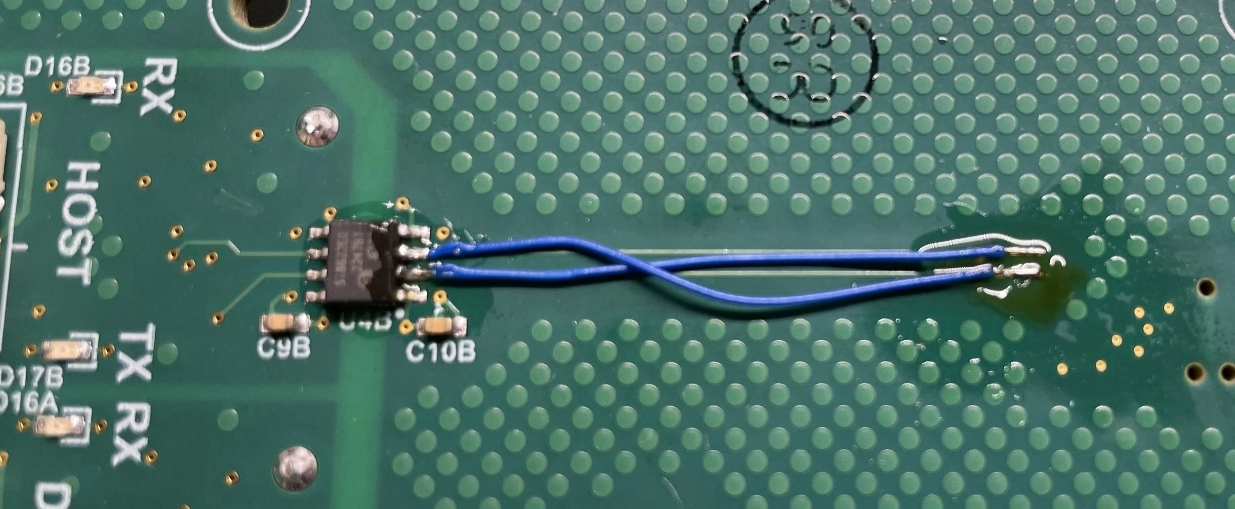
Many errors —the design engineer’s or a manufacturing/assembly error— can be fixed easily with a scalpel and kludge-wire. If you’re lucky, most of the time is spent finding the error, and the kludge-wire fix is fairly simple and quick.
In this example with the two kludge-wires, it was one of the most frequent and easy mistakes to make: getting the TX and RX signals of a serial interface the wrong way around 🤦🏻♂️. Why is this kind of error so common? Because TX (transmit) and RX (receive) are concepts applied to each chip at either end of a serial connection; the transmit-output of one chip should go to the receive-input of the other chip. If you get them the wrong way around, the transmit of one is connected to the transmit of the other (not only are they basically ‘shouting’ at each other and neither is listening, but they may even damage each other!), but they’re also deaf, both RXs listening to each other on the same silent piece of string - d’oh!
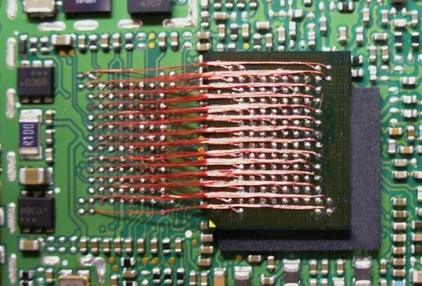
Some errors can be quite fundamental, often major forehead-slappers like the one pictured here, where the footprint of a BGA chip with 100 pins was apparently laid out with all the pads in the wrong order along one axis (“OMG, how did I get that entire footprint flipped left-to-right!?🤦🏻♂️”). In this example (thankfully not mine!), because of the complexity and cost of the just-manufactured PCBA, it can sometimes be economical for the at-error engineer to spend a day, or even a week, applying daunting amounts of kludge-wire fixes with very fine tools and steady hands, to every PCBA, rather than fixing the eCAD error and sending it off for a whole new spin.
Unfortunately, as serial bus speeds rise to ever faster frequencies and rise/fall-times, this kind of remedy is a shrinking option, because of the required signal integrity of ever-higher-speed serial buses; even if the kludge-wires corrected the basic electrical connectivity error, the additional length of those kludge-wires could render the chip inoperable, or at least unreliable.
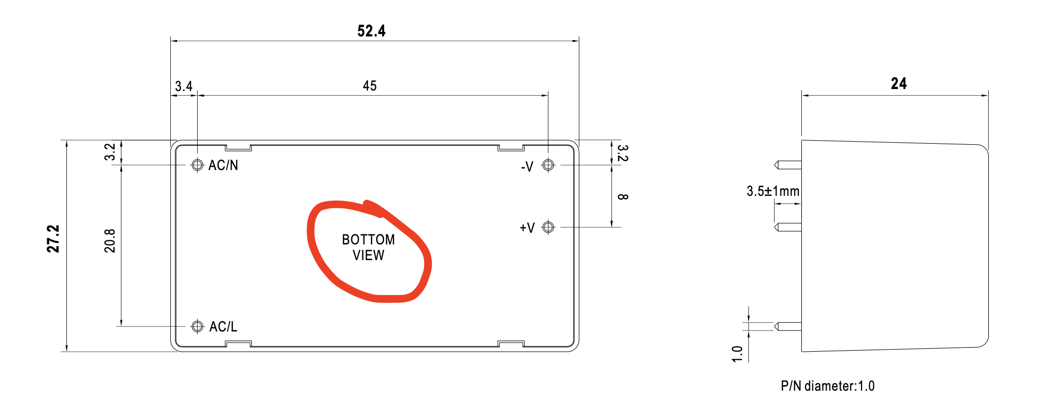
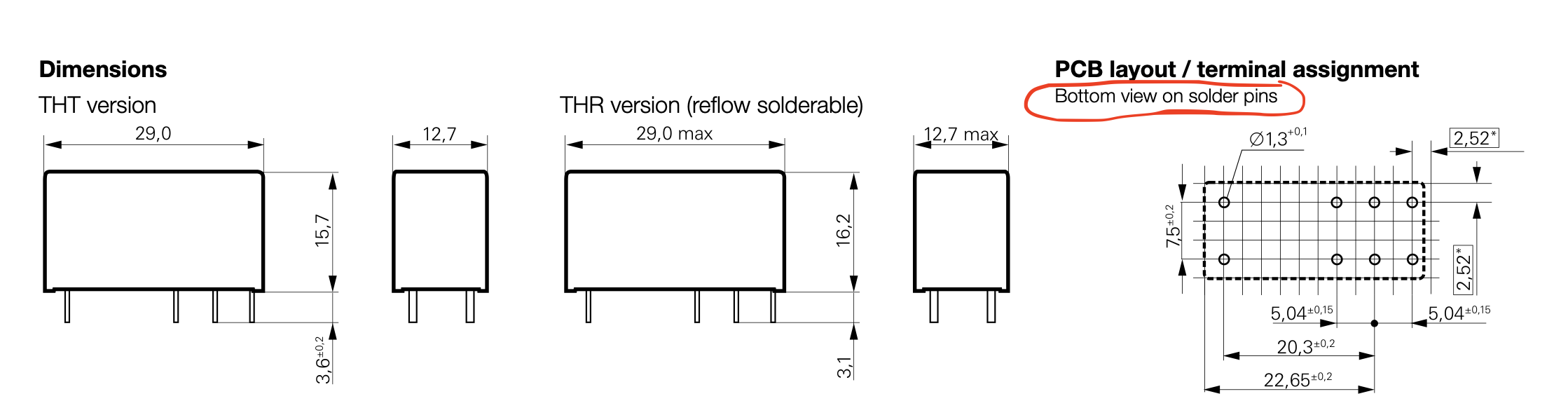
Unlike most electronic component vendors who show footprints in their datasheets looking from the top of the component (viewed as though the component itself were transparent other than the ‘footprints’ of its pins/pads), some categories of component vendors show footprints looking from the bottom-up, like turning over a turtle to inspect its belly. Like some relay and power-conversion module manufacturers! 🤬
Why? I’m not sure. In the case of relays, perhaps it’s because “that’s how we’ve drawn our diagrams for the past century, so why change now?” 🤦🏻♂️, but DC-to-DC and AC-to-DC power conversion modules are a much newer product category, so I don’t know what their reasoning could be. If you know, please let me know in the comments!
Despite the datasheet examples I show clearly inform you this is a bottom view, when 99% of datasheets you read show footprints looking from top down through the component, it’s still so easy to not see this and assume a top view.
Thankfully, in this example of an inverted footprint, the engineer who reviewed my work caught the error; years later, I, in turn, saved a client’s spin from exactly the same type of error by reviewing their Senior EE’s project just before it was to be sent for manufacturing. That spin was intended to be a near-public-release prototype run of 50 PCBs intended for field testing, costing at least $10,000, all of which would’ve been a write-off had the error not been caught in Design Review. For less than a tenth of that price, my client’s $10,000 investment was nailed, Right First Time.
If the error is severe enough that not even a kludge-wire hack will fix it and the PCBA is a useless write-off, what follows is the gut-wrenching realisation that I need to go back to the eCAD, fix the design mistake, or contact the fabricator or assembler and discuss the manufacturing error in detail, and ultimately send that design off for a whole extra spin, and you doubting your faith in me.
The cost. Another few weeks of waiting. Another few weeks later to market.

A Showstopper, Discovered Too Late!
Sometimes you don’t even have to wait for the PCBA to return from the Assembler and commence bring-up testing. Suppose I happen to take another look at the eCAD for that PCB during this eternal infernal wait. I might find something I want to change, minor tweaks mostly, and that’s okay although those changes won’t make it into production until the next spin, whenever that will be…
But on rare occasions (thankfully only once in my career so far!), I see something truly horrible I’d missed until now, a show-stopper in the design that’s currently winding its way through two dozen manufacturing steps! 😱
In that horrible moment, I realise I’d screwed up big-time, probably weeks or even months ago. The hundreds/thousands/tens-of-thousands of $€ you’ve just committed to this spin will at least in part be wasted. I’ll have to call the Fabricator with a lump in my throat and say, “Ummm, hi, my job# X, ummm, sorry, but you’re going to have to stop it (and throw some or all of it out) because I just discovered a show-stopper design error”.
“OK, no problem.” they respond. Of course it’s no problem for them, it’s another $ka-ching$ for them! Then I’ll have to tell you, my client, I just screwed up in a way that will cost a lot of extra dollars/euros 🤦🏼♂️
Why Am I Telling You All This?
I assure you I’m not trying to scare you off designing products involving electronics! 😂 If my honesty makes you worry about my abilities, I’m telling you things most engineers try to avoid mentioning in such candid terms, even though they’ll quietly admit all this is “normal”. I believe my clients are best placed to evaluate their risk profile and realities, as determined by funding/costs, development timeline, and other factors outside my purview. Forewarned is forearmed.
If you’re a hobbyist, or getting three prototype PCBs fabricated and assembled at JLCPCB/et.al. for $33 including shipping in 7 days, then sure, you probably don’t need to be this rigorous!
For everyone else, the one simple message I’m conveying in this recent series of posts is the critical importance of doing all the things that we know, from hard-won experience, will dramatically increase the probability of a Right First Time spin:
small-scale focussed prototypes
designing electronics with ‘battle tested’ eCAD libraries
having the design - all of it - thoroughly reviewed by a dispassionate independent engineer
…and get it Right First time!
Sign up for The Second Spin blog for more articles like this!
Happy spins!
Anthony.