
Empathy-Driven Development
A long time ago an episode of one of my favourite podcasts, Embedded.fm, interviewed Chris Svec (Director Of Software Engineering, iRobot), who has given presentations around the idea of Empathy-Driven Development. The term is a word-play on the software development paradigm Test-Driven Development, where he talks about the need to write code and documentation with empathy for those people who come after you, or for yourself months and years later when you need to revisit a codebase.
Who Is Documentation For?
Experience has repeatedly shown me that empathy for the viewers and inheritors of my electronics designs and documentation is important because they will have a wide range of electronics experience. They’re also usually looking at the schematic to answer a question as quickly as possible.
In the employer/employee situation, churn constantly erodes institutional knowledge leading to institutional amnesia. From my random sampling of the internets, the median tenure of EEs is only 2 years! 😱
The detail in the schematics I design departs my head within months, a year at best. After that, I’m almost coming in as fresh as someone who’s never seen it before! And what if I’m run over by a 🚌?!
Sooner or later, someone else will have to pick up my design and run with it:
my client’s growing business has new EE staff performing the next spin
they fork the design toward a whole new product
they have it manufactured somewhere new
they’re now manufacturing so many units of the product they need to hire more production staff, who must understand how this design works to test it, program it, assemble it, and fix it.
After my involvement, many people will need to ‘consume’ my design documentation.
These are all the consequences my clients face when they succeed, and everyone downstream from me benefits greatly from understanding my design & documentation quickly and with technical accuracy.
A Tale Of Two Schematics
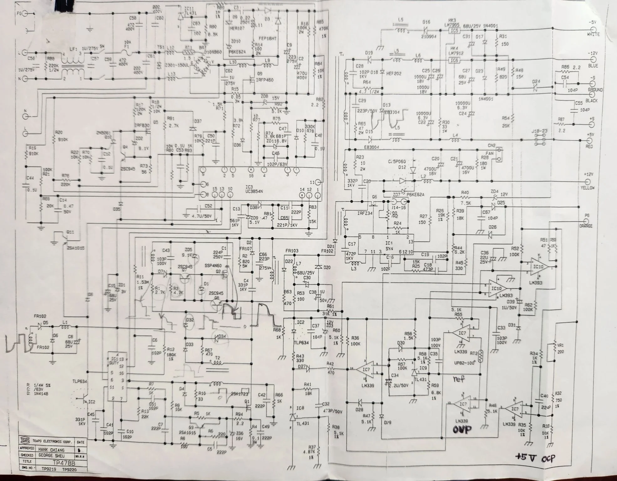
One of the first things a newcomer to an electronics design will see is the schematic diagram. Which of these two schematic diagrams best conveys design intent: the one on the left or the one on the right?
They’re functionally identical, but in my opinion, only one clearly conveys the designer’s intent.
The schematic on the left employs a modern, popular approach to schematic design, but one I think is horrendously overused: isolated blobs of circuitry linked with NetLabels (those are the words in dark red sitting on lines—aka wires, aka tracks on the PCB—that can be used to link two or more points in a circuit without actually drawing a line on the schematic).
Every time I’m confronted with the schematic style on the left, I’m repeatedly asking “Does this NetLabel only go to one other place, or two, or more!?” I can’t tell until I search the whole damned schematic! 🤬
I despise this approach; it’s actively hostile to the new viewer who’s expected to ‘wire up’ the schematic in their head! It’s a completely unnecessary additional cognitive load put upon everyone who comes to read the schematic to answer their question. Not every person new to the schematic will have the eCAD software to be able to click on a node to highlight all the places where that node connects; they’re often likely to be viewing a PDF, or maybe even on paper!
Techydude’s Style Guide:
Sections of circuitry should be linked with lines - wires - wherever it’s sensible to do so. Sure, if there are too many, it will clutter the page even worse, so judgment is required. Some connections are much more important to show with lines/wires than others. You can have lines without introducing clutter by carefully placing all those blobs of circuity on the page logically and thoughtfully, and that, in turn, might hugely benefit by changing the pin arrangement of the major ICs - move those pins around to meet closest to where those blobs of peripheral circuitry are! Remember, the schematic is a logical design document; it’s not meant to echo the geographic layout of the pins on the physical IC! (Doing so is a compromise to help beginners bridge the gap between logical and physical)
If the schematic is complex enough to need multiple pages, then, of course, use those more advanced connectivity drawing tools (ports, buses, harnesses, etc) where signals go to other pages, &/or multiple signals are contained in a single line on the page. Altium’s hierarchical design and multi-page features are excellent and flexible.
NetLabels shouldn’t be too long, but long enough to convey meaning to a fellow EE without spending more than a few seconds guessing. If you have multiple sets of similarly named signals (e.g. multiple SPI buses), then put a ‘key’ in a text-box explaining what each NetLabel prefix/suffix is for (e.g. what each SPIbus is for).
Colour! Damn Altium and their pale-yellow-box for everything! We can do so much better than hand-drawn black pen on white paper like the cover image for this post! Colour is an under-utilised tool in schematics to complement the conveying of design intent in schematics: categorisation, structure, demarcation. Even most people with some form of colour-blindness will be able to see colours, just not the full range, or certain colours will be hue-shifted. So this isn’t completely wasted on them if the colour scheme isn’t carrying any unique information.
I adopt a colour scheme for various component and documentation types:
ICs: Yellow
Connectors: Green
Jumper-headers: Grey
Text Note Boxes: Blue
Galvanic Isolation: Dashed-green lines and explanatory notes in green boxes
I often leave myself ’TO-DO’ notes scattered over the schematic in its early stages or during re-design. I add them as soon as something occurs to me, and they remind me later that there’s something incomplete; just plain red text on a single line. Sure, you can add Notes, but because Altium 365 uses them for collaborative commenting amongst a team, they don’t quickly convey the subtext “Note to Self: This is yet to be done! Don’t forget to do it before the next release!’.
Every schematic sheet Title Block should have the minimum details for anyone to be certain of what they’re looking at at any point in the future:
Company / Client Name (or Client-Code)
Project/Product Name (or Code)
Designer’s & Reviewer’s Name or Initials
Schematic Revision Number/Letter
Release Date of this revision
Page X of Y-total-pages
Passives should have all the relevant parameters listed on each component. Capacitors, for example, should have not only Designator and Capacitance but also Voltage and Dielectric, and maybe Package, too, if it’s relevant. Or, if the majority of such components are all the same in the design, then a sweeping “All capacitors are 0402 25V X7R unless otherwise noted” in a Text Box, for example, or “All decoupling capacitors are…”.
The purpose of a schematic diagram isn’t only a necessary step to designing a PCB, but also to help other humans understand your design intent. Empathy goes a long way and costs little. It isn’t just for unspecified other people (remember, you will be that other person too, one day, when picking up someone else’s designs); it’s also for yourself in the not-too-distant future!
Sign up for The Second Spin blog for more articles like this!
Happy spins,
Anthony.
FOOTNOTE-1: The original design shown in my two side-by-side examples is open-source, I downloaded it from the designer’s Github, imported it into Altium, then re-laid it according to my style guide. I won’t identify the designer here, it’s not relevant and my point is not to criticize this designer personally; as I said, the style has become very common.